Advanced Patterning for Enabling
Next‑Generation Devices As device geometries shrink, the complexity of patterning required to create the template that defines the features of a device is growing. Patterning approaches have shifted from lithography-reliant bidirectional to unidirectional, with the number of deposition and etch steps increasing significantly.
Next‑Generation Devices As device geometries shrink, the complexity of patterning required to create the template that defines the features of a device is growing. Patterning approaches have shifted from lithography-reliant bidirectional to unidirectional, with the number of deposition and etch steps increasing significantly.
The animations below illustrate some of the challenges encountered and state‑of‑the‑art patterning techniques used in creating today’s leading‑edge devices.
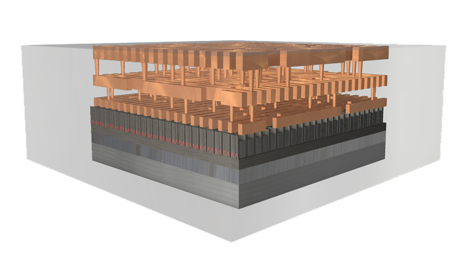

Patterning Technologies
and Device Scaling
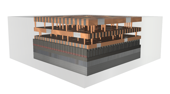
As we progress from 14 to 7nm devices and beyond, SADP and SAQP will be required for some layers and LE with either 193i or EUV lithography for others.
and Device Scaling
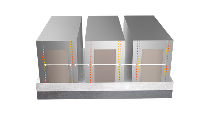
Pitchwalking
SAQP Eases
Litho Resolution
Self-aligned quadruple patterning effectively decreases the lithography resolution by 4x using a spacer-based patterning approach with one lithography step and two spacer depositions.Litho Resolution
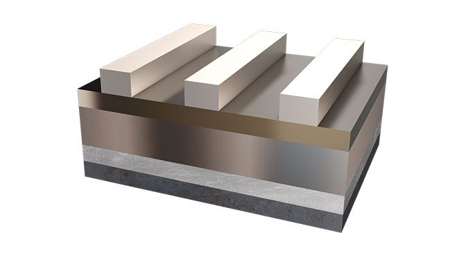
Multiple Litho/Etch Creates
High‑Density Cuts and Vias
To cut lines and create vias at densities too high to achieve in one pass, several iterations of lithography and etch are used.High‑Density Cuts and Vias
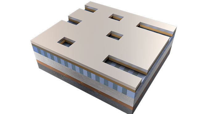
Multi-Color Patterning
Minimizes Edge Placement Error
Multi-color patterning is a materials-based approach that minimizes EPE, which is the undesirable movement of an edge in any direction, resulting in shorts, opens, and reduced reliability. Minimizes Edge Placement Error
SUMMARY
Self-Aligned Multi-Patterning and materials engineering will be major contributors to minimizing EPE, the most critical factor limiting scaling. In the future, 80% of the patterning market will depend on materials‑enabled solutions.
With our breadth and depth of capabilities in materials engineering, Applied Materials systems can address the variations leading to pitchwalking and EPE, thereby enabling the fabrication of the semiconductor industry’s most advanced devices.